NVIDIA Rubin Ultra AI Chip May Deliver Less HBM Than Rubin, Forcing Procurement Replanning
Resumo
NVIDIA está avaliando quatro configurações de memória HBM diferentes para seu chip Rubin Ultra AI de 2027, incluindo opções que reduziriam a memória de 288GB para 192GB devido à escassez estrutural de DRAM esperada em 2027, forçando replanejamento de compras da indústria.
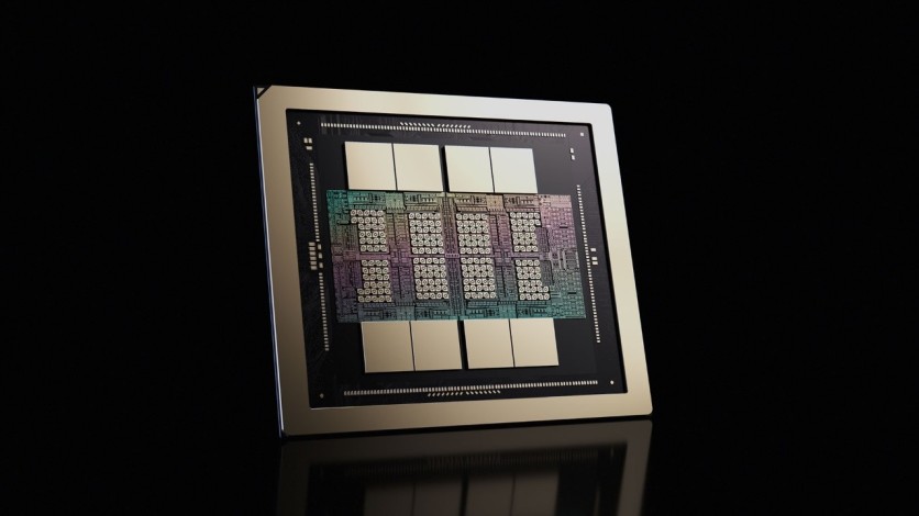
The AI chip NVIDIA has spent the last two years positioning as its 2027 performance crown may arrive with less on-package memory than the chip it is designed to supersede. A TrendForce market intelligence report published August 4 revealed that NVIDIA has begun evaluating four separate High Bandwidth Memory configurations for its Rubin Ultra AI accelerator — including options that would reduce the chip to 8-Hi HBM4, a specification that research firm SemiAnalysis says yields just 192 gigabytes of on-package memory. That figure is 33 percent below the 288 gigabytes carried by the current Vera Rubin GPU, meaning the platform branded "Ultra" could reach customers with a meaningful memory step backward relative to its own predecessor.
The finding is not a design failure in the traditional sense. It is a supply failure with design consequences. DRAM scarcity — the structural shortage that has compressed memory availability across every tier of computing since 2024 — has now reached the threshold where it is writing the specification of the world's most anticipated AI chip, not merely constraining the price at which that chip is sold.
Four Options Where There Was Once One
Since the third quarter of 2026, NVIDIA has expanded its evaluation of Rubin Ultra's HBM configuration beyond its original 12-Hi HBM4E design to include 8-Hi HBM4E, 12-Hi HBM4, and 8-Hi HBM4 alternatives. The final specification has not been determined. NVIDIA maintained 12-Hi HBM4E as the baseline design for Rubin Ultra from 2025 through the first half of 2026; the broader evaluation began in early Q3 2026 and is driven by two supply-side constraints: the overall DRAM shortage expected in 2027 will limit the wafer capacity that memory suppliers can allocate to HBM production, and uncertainties remain regarding the validation schedule and production yield ramp-up for 12-Hi HBM4E specifically, according to TrendForce's August 4 report.
SemiAnalysis, the semiconductor research firm, reported separately that the picture may already be more definitive than TrendForce's four-option framing suggests. The Rubin Ultra's mainstream SKU will still use HBM4 — with peak theoretical FLOPs unchanged — but its HBM configuration has been reduced to 8-Hi and 192 gigabytes, down from the current Rubin's 12-Hi and 288 gigabytes. NVIDIA has not confirmed either finding publicly.
Ultra in Name Only: Why 192GB Is Less Than Rubin's 288GB
The comparison that matters here is not between what Rubin Ultra will deliver and what was promised at GTC 2026. It is between what Rubin Ultra may deliver and what the non-Ultra Rubin already does.
The current Vera Rubin GPU, which entered full production in June 2026, carries 288 gigabytes of HBM4 in a 12-Hi stack configuration, providing 22 terabytes per second of aggregate memory bandwidth across eight stacks. The SemiAnalysis scenario — 8-Hi HBM4 in the same eight-stack configuration — would produce 192 gigabytes. That is a 96-gigabyte reduction per GPU relative to the chip Rubin Ultra is supposed to improve upon.
The mechanism behind this comparison is the HBM stack-height tradeoff. Within a single HBM generation, reducing the number of DRAM die layers per stack — from 12-Hi to 8-Hi — cuts memory capacity per stack by approximately one-third. Each DRAM die must be thinned to roughly 50 micrometers to achieve the 12-Hi stack height currently in production for Vera Rubin. An 8-Hi stack requires fewer thinning passes and fewer through-silicon via interconnections per stack, making it significantly easier to manufacture at high yield — which is exactly why it becomes attractive when wafer allocations are constrained. Fewer layers per stack means fewer gigabytes per GPU but more GPUs shipped from the same total wafer input. As TrendForce notes, within a given generation, the number of DRAM stack layers determines the tradeoff between HBM capacity per GPU and the number of GPUs that can be shipped.
Bandwidth at Stake: The I/O Speed Gap That Determines AI Throughput
The choice between HBM4 and HBM4E is a bandwidth question with direct consequences for AI workload throughput, not only a capacity question.
Whether HBM4E completes validation and enters mass production on schedule will determine whether Rubin Ultra's I/O speed can be raised from the previous-generation Rubin's 8–11.7 gigabits per second to 14–16 gigabits per second, or whether it will only reach 11–12 gigabits per second through HBM4 design optimization, according to TrendForce's August 4 report. That range — 11–12 Gbps under the HBM4 scenario vs. 14–16 Gbps under HBM4E — represents approximately a 25–35 percent I/O speed gap.
For large language model inference, memory bandwidth is frequently the binding constraint on throughput. A GPU that achieves only 11–12 gigabits per second per pin when its buyers planned around 14–16 will deliver proportionally lower token output on bandwidth-sensitive inference workloads. Enterprise customers deploying Rubin Ultra for large-scale inference should treat the HBM specification as a key procurement variable, not a settled technical fact, until NVIDIA makes a public disclosure.
HBM4E doubles the per-pin data rate of HBM4 through a higher-voltage physical layer interface and enhanced signal conditioning. HBM4 was standardized in April 2025 at up to 8 gigabits per second per pin across a 2,048-bit interface, delivering up to 2 terabytes per second per stack. HBM4E, the enhanced variant, raises that target to 14–16 gigabits per second per pin — delivering up to 4.1 terabytes per second per stack — by operating the same 2,048-bit interface at a significantly higher data rate. The per-stack bandwidth advantage compounds across the eight stacks on a single Rubin Ultra GPU, translating the per-pin difference into a substantial aggregate throughput gap at the chip level.
Supply Pressure: Why This Is the Third Compression in Six Months
The Rubin Ultra HBM evaluation did not arise in isolation. TrendForce has documented a pattern of supply-driven specification reductions across the platform that now spans three distinct memory subsystems.
Server OEMs and cloud service providers reduced RDIMM capacities for server configurations during the first half of 2026 as the broader DRAM shortage tightened available supply. Then, more recently, NVIDIA decided to halve the SOCAMM capacity of its next-generation Vera Rubin Superchip modules after determining that LPDDR5X supply constraints are likely to continue through 2027 — reducing the default configuration from 192 gigabytes to 96 gigabytes per Vera CPU slot. And now, the HBM specification itself is under review. Taken together, this is not a series of isolated engineering adjustments; it is a pattern in which supply scarcity is consistently choosing NVIDIA's specifications on its behalf.
HBM bit shipments are projected to grow by 50–60 percent year-over-year in 2027, but TrendForce's HBM supply analysis shows that rate will still be insufficient to keep pace with demand growth. Under those conditions, HBM suppliers are expected to retain pricing power throughout 2027, with significant pricing increases already widely anticipated. AI chip vendors will face the dual challenge of both limited HBM supply and higher procurement costs — increasing the incentive to adopt lower-capacity HBM configurations, according to TrendForce.
The constraint behind all of this is structural. HBM requires approximately three to four gigabytes of standard DRAM wafer area to produce one gigabyte of HBM output. At the same time, HBM generates three to five times the revenue per wafer of commodity DDR5. Manufacturers allocate toward HBM because the economics demand it — and every wafer running HBM is three to four wafers not running conventional DRAM. New fab capacity commissioned today is not expected to produce meaningful output until 2028 at the earliest. Samsung's P5 megafab in Pyeongtaek targets mass production in the latter part of 2028; SK Hynix's M15X facility is slated for initial utilization by mid-2027.
Why Does HBM4E Qualification Matter So Much?
The second driver of the Rubin Ultra review is specific to HBM4E's manufacturing maturity. SK Hynix confirmed in June 2026 that it had delivered 12-layer HBM4E samples to major customers ahead of its previously stated second-half timeline, and is working closely with customers to reach mass production on schedule. But delivering samples and reaching qualified, high-yield mass production at 12-Hi stack height are materially different achievements.
Twelve-Hi HBM stacks are extremely complicated to fabricate. Industry observers have described formidable manufacturing challenges at scale for higher stack counts, with thin wafer thickness the central concern. Each DRAM die must be thinned to approximately 50 micrometers before stacking; the uniformity of that grinding process across billions of dies at production scale is what determines yield. For HBM4E specifically, achieving 14–16 gigabits per second per pin at 12-Hi stack height requires not only the physical stacking to work, but the high-speed PHY interface to perform reliably at those elevated data rates across the full production spectrum. Until validation is complete and yield ramps sufficiently, the 12-Hi HBM4E option remains uncertain for 2027 volume production.
Does Cloud Infrastructure Need to Worry?
Several cloud service providers are also evaluating lower HBM capacities for their next-generation in-house AI ASICs, indicating the pressure is not exclusive to NVIDIA. Hyperscalers including Google, Microsoft, Meta, and Amazon have been developing proprietary AI accelerators that compete for the same HBM supply as NVIDIA's products.
TrendForce believes the final Rubin Ultra configuration will depend on wafer allocation decisions made by memory suppliers — meaning the chip's specification is being determined in part by the fabs, not solely at NVIDIA's headquarters. That dynamic is unusual for a company accustomed to dictating the terms of AI hardware at every generation. NVIDIA and SK Group announced a $500 billion-plus strategic partnership on July 25, 2026, covering long-term HBM4 co-development, a deal structured precisely because locking in priority allocation requires a multi-year commitment that smaller customers cannot make.
What Memory Suppliers Gain and Lose
The specification evaluation creates divergent outcomes among the three major HBM producers. A large-scale shift in the Rubin Ultra baseline away from HBM4E would meaningfully reduce the share of HBM demand that requires the more technically demanding — and higher-margin — HBM4E product. TrendForce has forecast that HBM4E will account for approximately 40 percent of overall HBM demand in 2027. A broad Rubin Ultra downgrade to HBM4 would revise that share downward, with downstream consequences for supplier revenue mix and the per-gigabyte premium that HBM4E commands over standard HBM4.
The impact would not, however, reverse the underlying DRAM price trajectory for 2026. The constraints driving HBM4E demand reduction are the same ones that keep DRAM broadly undersupplied. SK Hynix CEO Kwak Noh-jung stated publicly that 2027 supply will be historically worst in the industry's history, and Micron CEO Sanjay Mehrotra has indicated that supply tightness persisting beyond 2027 is the company's base expectation. A reduction in HBM4E content per Rubin Ultra GPU softens the slope of potential price increases but does not flip the market direction.
What This Means for 2027 AI Infrastructure Planning
The unresolved question heading into the second half of 2026 is whether 12-Hi HBM4E can clear NVIDIA's qualification bar in time to restore the original specification before production commitments are locked. If it does not, Rubin Ultra — once positioned as a substantial leap in memory bandwidth over its predecessor — may arrive with a more modest upgrade story than the AI hardware market expects.
Enterprise customers and hyperscalers evaluating 2027 infrastructure deployments face a procurement environment where the flagship chip's specification is still being decided by forces outside the chip designer's control. The practical implication is clear: buyers who have based workload sizing, rack count estimates, or token cost projections on 384 gigabytes per GPU need to build contingency models around 192 gigabytes per GPU and 11–12 gigabits per second of I/O speed. A chip that delivers less on-package memory than the current Rubin, at lower bandwidth than HBM4E would provide, is not the chip that was evaluated in 2025 planning cycles. Updating those models now — before production commitments lock — is the decision that this reporting makes possible.
Frequently Asked Questions
Why might Rubin Ultra ship with less memory than the regular Rubin GPU?
The HBM stack-height reduction — from 12-Hi to 8-Hi — is driven by two intersecting supply pressures, per TrendForce's August 4 report. First, the structural DRAM shortage expected to peak in 2027 limits the total wafer capacity that memory suppliers can allocate to HBM production. Second, the 12-Hi HBM4E configuration that was originally specified for Rubin Ultra has not yet completed qualification and production yield ramp-up. Within a given HBM generation, reducing from 12-Hi to 8-Hi cuts memory capacity per stack by approximately one-third — but it significantly improves manufacturing yield and allows more GPUs to be shipped from the same wafer input. That tradeoff is what NVIDIA is now being forced to evaluate.
What is the difference between HBM4 and HBM4E, and why does it matter for AI workloads?
Both HBM4 and HBM4E use a 2,048-bit wide interface — twice as wide as HBM3 — but they differ on per-pin data rate. HBM4 reaches 8–11.7 gigabits per second per pin in current production; Rubin Ultra with optimized HBM4 could reach 11–12 Gbps. HBM4E is designed to reach 14–16 Gbps per pin through a higher-voltage physical layer interface, delivering up to 4.1 terabytes per second per stack versus roughly 2 terabytes per second for HBM4. For large language model inference, where memory bandwidth is frequently the binding constraint on how many tokens the GPU can process per second, the 25–35 percent I/O speed gap maps directly to throughput. Buyers running bandwidth-sensitive inference workloads should treat the HBM specification as a material performance variable.
How does the HBM stack-height tradeoff work technically?
Each HBM stack consists of individual DRAM dies stacked vertically and connected by through-silicon vias — microscopic copper pillars drilled through each die. A 12-Hi stack uses 12 DRAM dies; an 8-Hi stack uses 8. Each die must be thinned to approximately 50 micrometers before stacking, and achieving reliable through-silicon via alignment across all layers at production scale is what makes higher stacks progressively harder to manufacture. Reducing from 12-Hi to 8-Hi cuts per-stack memory capacity by roughly one-third, but it meaningfully reduces the yield challenge — and because HBM requires three to four times the wafer area of conventional DRAM per bit produced, making each stack easier to build means more GPUs reach customers per wafer allocated. That economic pressure, compounded by the DRAM shortage, is what makes the 8-Hi option increasingly attractive even though it produces a lower-specification chip.
What should enterprise IT and cloud infrastructure buyers do right now?
Any 2027 AI infrastructure plan that was sized around 384 gigabytes of HBM per Rubin Ultra GPU needs to be revisited. The most prudent approach — given that neither TrendForce nor SemiAnalysis has confirmed which of the four candidate configurations will ship — is to build parallel models: one at 288 gigabytes (parity with Rubin), one at 192 gigabytes (the SemiAnalysis mainstream scenario), and one at 384 gigabytes (the original spec, which remains possible if HBM4E qualification succeeds). Rack counts, network bandwidth requirements, and per-token cost projections differ substantially between these scenarios. NVIDIA has not made a public disclosure; buyers relying on the chip's currently published specification are working from a roadmap that supply constraints have already revised at least twice in the past six months.
ⓒ 2026 TECHTIMES.com All rights reserved. Do not reproduce without permission.