TSMC Revives Longtan for 1.4nm Fabs and CoWoS Hub as Both Sell Out Globally
Resumo
TSMC planeja construir dois a três fabs de 1.4nm e duas unidades de empacotamento avançado em Longtan, Taiwan, criando a maior concentração de capacidade de semicondutores de última geração do país, com conclusão não antes de 2029.
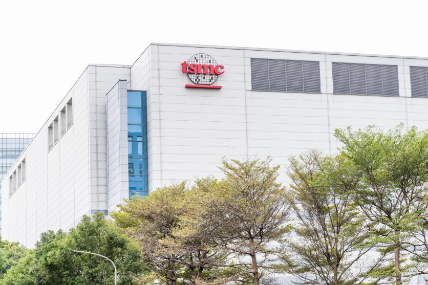
Taiwan's most watched domestic semiconductor land deal is back on track. After residents of Longtan, a district in Taoyuan in northern Taiwan, reversed their opposition to the area's third-phase science park expansion, TSMC is now planning to build two to three next-generation 1.4nm fabrication plants alongside two advanced packaging facilities at the once-rejected site — making Longtan Phase 3 the only location in the world currently planned to house both technologies under construction simultaneously, at the moment both are globally sold out.
The five-facility plan, reported by supply chain sources cited by Liberty Times, would create what analysts describe as the densest concentration of cutting-edge semiconductor capacity Taiwan has built since the original Hsinchu Science Park cluster took shape decades ago. The site faces substantial remaining hurdles — an Executive Yuan review is ongoing, an environmental impact assessment has not yet cleared, and land acquisition from predominantly private landowners will not be completed until 2029 at the earliest. But the direction of travel has shifted decisively from 2023, when TSMC walked away entirely.
How Longtan Went From Abandoned Plan to Government Priority
The story of Longtan Phase 3 is, in miniature, the story of what happens when a government is unwilling to accept a chipmaker's "no."
When Taiwan's government first unveiled the Phase 3 expansion of Longtan Science Park in late 2022, it ignited a backlash from local landowners who opposed the compulsory acquisition of their privately held plots — around 88 percent of the targeted land is in private hands. A self-help group representing residents accused the government of steamrolling communities in the name of industrial growth. Coverage in the Taipei Times documented resident protests and the residents' demand that the land acquisition plan be scrapped entirely.
By October 2023, TSMC had reached its limit. The company issued a statement saying it was "no longer considering establishing a site at phase 3 of the Longtan section under present conditions," effectively shelving what had been its most anticipated domestic factory announcement. Digitimes confirmed the withdrawal on October 17, 2023. The chipmaker pivoted south, deepening investments in the Southern Taiwan Science Park in Tainan and Kaohsiung, where its 2nm production is now ramping at Fab 22.
But the Hsinchu Science Park Bureau — the administrative body overseeing the park — kept working. In late 2025 and early 2026, it held two rounds of public hearings on the third-phase expansion. Village chief Ye Laiwang publicly expressed willingness to support development, citing the employment and educational benefits a major technology cluster could bring. Political representatives pushed for updated urban plans to address infrastructure deficiencies that had accumulated in some cases over nearly 50 years. The Taipei Times confirmed community reversal, with many affected residents now warming to the TSMC fab plan.
With opposition softening, the bureaucratic machinery accelerated. The Hsinchu Science Park Bureau submitted the Phase 3 proposal to Taiwan's National Science and Technology Council in May 2026, and the council approved it that month. The plan was then forwarded to the Executive Yuan in June for further review — a step that remains outstanding as of today. Focus Taiwan / CNA confirmed the NSTC submission and TSMC's non-denial of the angstrom-class development plans.
What TSMC Would Build — and Why Both Technologies Matter Right Now
The specific mix of facilities TSMC reportedly plans for Longtan Phase 3 is not accidental. According to supply chain sources cited by Liberty Times, the campus would host two to three fabs built on TSMC's 1.4nm A14 process alongside two advanced packaging plants using CoWoS (Chip on Wafer on Substrate) technology.
Both are critically constrained right now, and that constraint is not separate problems but one interconnected one: you cannot build a functional AI accelerator chip without both.
The A14 process is TSMC's next major node after 2nm. Unveiled at the company's 2025 North America Technology Symposium, it uses second-generation nanosheet Gate-All-Around transistors combined with TSMC's NanoFlex Pro architecture, which allows chip designers to vary transistor channel width continuously rather than in discrete increments — a design freedom that prior-generation FinFET transistors could not provide. Compared to the 2nm node already ramping into production this year, A14 delivers a 10–15 percent speed gain at equivalent power or a 25–30 percent power reduction at equivalent speed, alongside roughly a 1.23x improvement in logic density. Volume production is targeted to begin at Taichung's Central Taiwan Science Park in mid-2028 — the Taichung fab's first building is now running ahead of its own construction schedule and is expected to be completed before April 2027, according to TrendForce and Commercial Times.
CoWoS is the packaging technology that connects the logic die to High Bandwidth Memory stacks sitting beside it on a silicon interposer — the intermediate layer that allows data to flow between the compute and memory at speeds and bandwidths that conventional 2D packaging cannot approach. Nvidia's Blackwell-generation GPUs require memory bandwidth exceeding 9,000 gigabytes per second; that throughput is physically achievable only if the logic and memory dies are separated by microns rather than millimeters, which only CoWoS accomplishes at production scale. As TechTimes has previously reported, CoWoS capacity is currently sold out through 2026 and well into 2027, with lead times running 52 to 78 weeks. Demand is expected to reach roughly one million wafers in 2026, nearly triple the approximately 370,000-wafer demand level across all of 2024. TSMC has been expanding CoWoS capacity at roughly 80 percent per year, but the gap between packaging supply and demand is only expected to narrow to approximately 10 percent by year-end, per TechTimes reporting on TrendForce data.
What makes Longtan Phase 3 structurally significant is that no single planned greenfield site anywhere in TSMC's current expansion program is designed from the ground up to house both A14 logic fabrication and CoWoS packaging in the same cluster. TSMC's Taichung Fab 25 will produce A14 but its dedicated packaging expansion is in Chiayi and Zhunan. The Arizona campus is targeting CoWoS capability around 2029 but will not manufacture A14 logic. Longtan Phase 3, if completed on its current planning horizon, would be the exception — the one site built to do both at the center of TSMC's original manufacturing corridor. TechTimes' global chip race coverage has documented why the U.S. packaging gap persists even after massive investment.
CoWoS at Longtan: Extending a Campus That Already Does This
Longtan is not new to advanced packaging. TSMC's existing Advanced Packaging Fab 3, located at the Longtan campus, already operates wafer-level multi-chip module and InFO packaging lines dedicated to high-end Apple processors, as detailed in Tom's Hardware's analysis of TSMC's fab expansion roadmap. The Phase 3 expansion's two new packaging plants would be built at the new, adjacent Phase 3 land — not at the existing Fab 3 site — and would likely support CoWoS, which bonds AI accelerator logic dies to HBM memory stacks rather than just stacking Apple chips.
At its April 2026 North America Technology Symposium, TSMC announced it is now producing CoWoS at 5.5-reticle size with yields exceeding 98 percent, while planning a 14-reticle version — capable of integrating approximately 10 large compute dies and 20 HBM memory stacks — for 2028, as TechTimes reported. A Longtan packaging hub, situated within the Hsinchu corridor close to TSMC's core R&D facilities, would be positioned to support that larger-scale CoWoS generation as AI chip designs continue to grow physically.
What Does It Cost, and What Would It Produce?
The site in question covers approximately 104 hectares (257 acres) in total, with around 46 hectares (114 acres) earmarked for industrial use. Land acquisition is targeted for completion by the end of 2029, at which point TSMC and other tenants could begin construction in earnest.
Supply chain sources cited in May 2026 reports estimated that TSMC could invest NT$500 billion to NT$600 billion (approximately $15.5 billion to $18.6 billion USD) into the angstrom-class project at Longtan, with the specific intent of keeping its most advanced technology development anchored in Taiwan, per Focus Taiwan / CNA. Taiwan Power Company has separately indicated it is preparing grid upgrades in anticipation of new industrial demand, with the Longtan campus expected to generate extraordinary power load once fully built out.
Earlier analyses estimated that a fully built-out Longtan Phase 3 could generate annual output valued at NT$600 billion to NT$650 billion (approximately $18.6 billion to $20.2 billion USD) and create around 5,900 jobs.
Taiwan's Domestic Anchor Logic
The revival of Longtan carries a geopolitical dimension that goes beyond the square footage. As TSMC accelerates international investments — with more than $65 billion committed to chip fabs in Phoenix, Arizona, and additional facilities in Kumamoto, Japan, and Dresden, Germany — Taiwanese policymakers have remained anxious to ensure the company's most advanced nodes stay rooted at home. TSMC CEO C.C. Wei has repeatedly affirmed that Taiwan will remain the base for the company's leading-edge production, as reported by TechTimes.
The three years of negotiation at Longtan — two rounds of public hearings, infrastructure commitments, urban planning revisions — represent what the Taiwanese government was willing to do to anchor a second domestic A14 site that it could not compel TSMC to build overseas.
Longtan occupies a singular position in Taiwan's semiconductor geography. The campus has hosted TSMC facilities since 2004, and its proximity to the Hsinchu corridor — home to TSMC's most advanced research and manufacturing — makes it a natural extension of the company's domestic cluster. The existing AP Fab 3 already serves Apple's most demanding packaging needs. Adding A14 logic fabs and new CoWoS capacity would transform the site from an advanced-packaging annex into a full-spectrum leading-edge hub.
What Is Still to Resolve
Not everything is settled. Environmental impact assessments and further Executive Yuan reviews remain outstanding before formal approval is secured. The land acquisition process — targeting 88 percent privately held plots — carries inherent complexity and will not conclude before 2029 under even optimistic projections.
A parallel boundary dispute adds another layer of uncertainty. Taoyuan City's government has been seeking to redesignate additional land around the park as an urban-rural development zone, a move that Taiwan's Spatial Planning Review Committee largely rejected, approving only the roughly 89 hectares already planned by the NSTC. The Taoyuan government resubmitted without revisions, leaving that boundary question unresolved, per the Taipei Times.
And the specific five-facility plan — two to three A14 fabs plus two CoWoS packaging plants — remains attributed to supply chain sources rather than official TSMC confirmation. TSMC has not confirmed the specific number of facilities planned for the site, stating only that it "does not rule out any possibility for new technology development" at Longtan while affirming Taiwan as its primary production base. Focus Taiwan / CNA confirmed the official TSMC statement.
Despite those open questions, the direction of travel is clear. After years of false starts and a bruising community conflict, Longtan Phase 3 has cleared its first major bureaucratic hurdles — and with it, the prospect of a cluster purpose-built for the chips and the packaging that AI infrastructure demands most.
All currency conversions use the exchange rate of August 9, 2026 (1 TWD = 0.031 USD; 1 USD = approximately 32.2 TWD) and are approximate.
Frequently Asked Questions
What is TSMC planning to build at Longtan Phase 3, and why does that specific combination matter?
According to supply chain sources cited by Liberty Times, TSMC plans to build two to three fabrication plants using its 1.4nm A14 process alongside two advanced packaging plants running CoWoS technology at the Longtan Phase 3 site in Taoyuan, Taiwan. The combination matters because it would make Longtan the only planned greenfield semiconductor site anywhere in TSMC's current expansion program designed to house both technologies under construction simultaneously. A14 is the process node that will power the next generation of AI accelerators after 2028, and CoWoS is the packaging step that connects those chips to high-bandwidth memory — the step currently bottlenecking AI chip supply, with lead times running 52 to 78 weeks and demand running roughly 10 percent above available capacity through year-end. Further context on A14's production timeline and CoWoS constraints is available in TechTimes' reporting on TrendForce data.
Why did TSMC abandon Longtan in 2023, and what changed to bring the plan back?
TSMC walked away from Longtan Phase 3 in October 2023 because local landowners — who hold roughly 88 percent of the targeted land — organized against the compulsory acquisition plan and the government's announced expansion. The company issued a formal statement that it was "no longer considering" the site under prevailing conditions, as Digitimes reported. What changed was a sustained negotiation effort by the Hsinchu Science Park Bureau, which held two rounds of public hearings in late 2025 and early 2026. Village leaders, including chief Ye Laiwang, publicly reversed their position, citing the employment and infrastructure investment the cluster would bring. With community opposition softened, the bureau submitted the expansion proposal to Taiwan's National Science and Technology Council in May 2026, which approved it. Focus Taiwan / CNA confirmed the submission and community turnaround.
What is CoWoS, and why is it sold out globally?
CoWoS — Chip on Wafer on Substrate — is TSMC's 2.5D advanced packaging technology that bonds a logic die and High Bandwidth Memory stacks onto a shared silicon interposer. The interposer acts as a microscopic circuit board that allows data to move between the compute die and memory at speeds impossible in conventional flat packaging. Every major AI accelerator on the market — Nvidia Blackwell and Rubin GPUs, AMD Instinct accelerators, Google TPUs — requires CoWoS to achieve the memory bandwidth their architecture demands. Because TSMC holds a near-monopoly on CoWoS production and because the interposer itself requires its own dedicated silicon fabrication line, there is no alternative source at scale for any chip designer that needs HBM integration. Demand in 2026 is expected to reach approximately one million wafers, nearly triple 2024 levels, while TSMC's capacity expansion can only narrow the gap to approximately 10 percent by year-end. TechTimes' advanced packaging coverage provides a full breakdown of the CoWoS constraint.
How does Longtan Phase 3 fit into TSMC's broader global expansion?
TSMC has committed more than $65 billion to chip fabs in Phoenix, Arizona, alongside facilities in Kumamoto, Japan, and Dresden, Germany. But none of those international sites is designed to manufacture A14-generation logic at volume while simultaneously operating CoWoS advanced packaging — the combination that makes a complete AI chip production cluster. Arizona is targeting CoWoS packaging capability around 2029 but will not manufacture A14 logic wafers. The Taichung Fab 25 in Taiwan will produce A14 but its packaging partners are elsewhere. Longtan Phase 3, if completed on schedule — with land acquisition running to 2029 and construction to follow — represents Taiwan's institutional attempt to anchor the full AI chip production stack, both logic and packaging, in the Hsinchu corridor that has housed TSMC's most advanced work since 1987. TechTimes' global chip race coverage and TSMC's A14 schedule provide further context.
ⓒ 2026 TECHTIMES.com All rights reserved. Do not reproduce without permission.